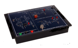
Advanced Digital Logic Lab
Description
Brand: PValley
Model: DL-622L9
Country of Origin: Bangladesh
Features:
- The whole trainer is fully designed by FPGA/CPLD logic circuit.,
- Buffer circuits have enhanced protection for each module which is powered by main unit through power socket,avoiding wrong input power source during the experiment.,
- Covers different levels of logic circuit experiments,ranging from combinational logic,sequential logic as well as the logic circuit interfacing with microcontroller and practical application circuit for daily use.,
- Students can implement their own circuit from universal CPLD& breadboard experiment module,making it possible to prototype most analog and digital circuits in the system.,
- Includes various types of ADC & DAC circuits to learn different interfacing circuits between analog and digital signal.,
- Built-in 8-channel multiplexer in main unit to measure multiple digital signals in real time.,
- Multiple operation modes from 4-digit 7-segment display
- (a)scanning display mode,
- (b) individual digit display mode,
- (c)frequency counter mode for measurement of internal and external clock.,
- Individual keep case for all modules for easy storing and carrying,,
- Specifications:
- Main Unit,
- DC Power Supply,
- Fixed DC power supply : +5V/2A,-5V/0.5A,+12V/2A,
- With overload protection,
- Clock Generator,
- (1)Signal amplitude output : 3.3V,
- (2)With adjustable output frequency : square wave,1Hz ~ 1MHz,6 range,
- (3)Frequency display :4-digit,7-segment LED,
- Logic Level Switch : Toggle switches x 8,3.3V output,
- Data Level Switch : 8-bit DIP switch x 2,3.3V output,
- Pulse Signal Generator,
- 2 sets of toggle switch with independent control output,
- Each set with Q,Qft output,
- Pulse width > 5ms,each with Denounce circuit,
- Logic Level Indicator,
- (1) 16-bit LED with driver and protection circuit,
- Input Impedance : > 100K ohms,
- 8 Channel Logic Signal Tracer,
- 8 logic signal input :input impedance : ≥ 100K ohms,3.3V input,
- Fixed DC level shift for each channel,
- Input signal attenuation ratio : 1/8,(4) Output signal : BNC or 2mm plug,
- Oscilloscope SYNC. select : ALT/CHOP and scan-frequency adjustment,
- The function can be used only with analog oscilloscope,
- 7-segment LED display & frequency measurement 2 DIP switches select the function :,
- 00 : Scanning display mode,
- Common anode for the control of 7-segments a ~ g,
- Scanning cathode for the control of 4-digit S0 ~ S3,
- 01 : Independent display mode,
- Input 4-digit of data individually and decode the data at 7-segment,display separately,
- Independent binary input and hexadecimal output,
- 10 : Frequency counter for internal clock,
- Display the frequency of clock generator from main unit,
- Frequency range : 0.001KHz ~ 999.9KHz,
- 11 : Frequency counter for external clock,
- Display the frequency of clock signal from external unit,
- Frequency range : 0.001KHz ~ 999.9KHz,
- Rotary Encoder,Rotary encoder output : PA,PB and GND signal,3.3V output,
- Standard Signal Generator,5 sets of frequency : 20MHz,1MHz,10KHz,100Hz,1Hz,,
- Experiment Modules,
- All built-in DC power socket module supply DC power from the main unit.,
- Each module includes a CPLD chip to implement all digital circuits shown on module panel.,
- 2mm sockets,bridgeplugs,and cables are used throughout all modules so that students can easily create the circuits and compare different results in short time.,
- With comprehensive experiment manual.,,
- List of Modules,
- Combinational Logic Circuit Experiment,
- Arithmetical Logic/Tri-state & Code Converter Experiment,
- Encoder,Decoder& Multiplexer Logic Circuit Experiment,
- Flip-flop & Sequential Logic & Counter Circuit Experiment,
- Oscillator/Pulser ; Load ; Up/Down Counter Circuit Experiment,
- Memory ; Matrix LED ; DAC/ADC & MCU Interface Circuit Experiment,
- Digital & Analog Timer,Pulse Generator Circuit Experiment,
- Ramp-compare/SAR/Dual-slope ADC Experiment
- List of Experiments,
- Combinational Logic Circuit Experiment,
- NOR gate circuit,
- NAND gate circuit,
- XOR gate circuit,
- Constructing XOR gate with NAND gate,
- The combination with basic gates
- AND-OR-INVERTER (A-O-I) gate circuit,
- Comparator circuit,
- Comparator constructed with basic logic gates,
- Comparator constructed with TTL IC,
- Schmitt gate circuit,
- Open-collector gate circuit,
- High voltage/current circuit,
- Constructing an AND gate with open collector gate,
- Half-adder and full-adder circuit Construct,HA with basic logic gates,
- Half-subtractor and full-subtractor circuit Subtractor,circuit constructed with basic logic gates,
- Bit parity generator circuit Bit parity generator,constructed with XOR gates,
- Constructing a 4-to-10 decoder with TTL IC,
- The switch characteristics of TTL level,conversion circuit,
- Arithmetical Logic/Tri-state & Code Converter,Experiment,
- CMOS FET tristate gate circuit,
- Truth table measured


Reviews
There are no reviews yet.