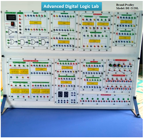
Advanced Digital Logic Lab
Description
Brand: PValley
Model: DE-2128L
Country of Origin: China
Features:
- The whole trainer is fully designed by FPGA/CPLD logic circuit.
- Buffer circuits have enhanced protection for each module which is powered by main unit through power socket, avoiding wrong input power source during the experiment.
- Covers different levels of logic circuit experiments, ranging from combinational logic, sequential logic as well as the logic circuit interfacing with microcontroller and practical application circuit for daily use.
- Students can implement their own circuit from universal CPLD& breadboard experiment module, making it possible toprototype most analog and digital circuits in the system.
- Includes various types of ADC & DAC circuits to learn differentiatefacing circuits between analog and digital signal.
- Built-in 8-channel multiplexer in main unit to measure multipledigital signals in real time.
- Multiple operation modes from 4-digit 7-segment display (a)scanning display mode, (b) individual digit display mode, (c)frequency counter mode for measurement of internal andexternal clock.
- Individual keep case for all modules for easy storing and carrying
General Specification:
Body Material:
Hard Round support board or Plastic Sheet
Sheet Type: Digital
Country of origin: Pakistan
Feature:
- Sheet thickness 6 mm
- Two-Part Combination(Transparent/white)
- UV Printout
Protection System
Feature:
- Safety tripping
- Low insertion loss and high reliability
Panel Box
Brand: Madhav Enterprise
Country of origin: Indian
Features:
- Shape: Rectangular
- Surface Finish: Smooth
- High quality raw material
Best structure
Brand: Altech
Country of origin: Bangladesh
Feature:
- Sheet thickness 5mm
- Square Shape
Power Supply
Brand: Fexcon
Country of origin: China
Feature:
- Output Voltage 5VDC
- Output Current 10000 mA
- Power Nature
- Input Voltage (100-250)VAC
Power Monitoring
Brand: UNI-T
Country of origin: China
Feature:
- Self-operating voltage 5V
- Self-Consumption Current 2500 mA
- Power Nature
- Two-row for Voltage & Current
Use Connector
Brand: ZHT
Country of origin: China
Feature:
- Banana Female Connector Diameter 4 mm
- Banana Male Connector Diameter 4 mm
Working area:
- Working area: 35*24 inch
Technical Specifications:
Main Unit
- DC Power Supply
(1) Fixed DC power supply : +5V/2A, -5V/0.5A, +12V/2A
(2) With overload protection
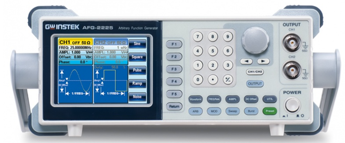
- Clock Generator
(1)Signal amplitude output : 3.3V
(2)With adjustable output frequency : square wave, 1Hz ~ 1MHz, 6 range
(3)Frequency display :4-digit, 7-segment LED
- Logic Level Switch : Toggle switches x 8, 3.3V output
- Data Level Switch : 8-bit DIP switch x 2, 3.3V output
- Pulse Signal Generator
(1) 2 sets of toggle switch with independent control output
(2) Each set with Q, Q’ output
(3) Pulse width > 5ms, each with Denounce circuit
- Logic Level Indicator
(1) 16-bit LED with driver and protection circuit
(2) Input Impedance :> 100K ohms
- 8 Channel Logic Signal Tracer
(1) 8 logic signal input :input impedance : ≥ 100K ohms , 3.3V input
(2) Fixed DC level shift for each channel
(3) Input signal attenuation ratio : 1/8
(4) Output signal : BNC or 2mm plug
(5) Oscilloscope SYNC. select : ALT/CHOP and scan-frequency adjustment
(6) The function can be used only with analog oscilloscope
- 7-segment LED display & frequency measurement 2 DIP switches select the function :
(1) 00 : Scanning display mode
a.Common anode for the control of 7-segments a ~ g
b.Scanning cathode for the control of 4-digit S0 ~ S3
(2) 01 : Independent display mode
a.Input 4-digit of data individually and decode the data at 7-segment
display separately
b.Independent binary input and hexadecimal output
(3) 10 : Frequency counter for internal clock
a.Display the frequency of clock generator from main unit
- Frequency range : 0.001KHz ~ 999.9KHz
(4) 11 : Frequency counter for external clock
a.Display the frequency of clock signal from external unit
- Frequency range : 0.001KHz ~ 999.9KHz
- Rotary Encoder:Rotary encoder output : PA, PB and GND signal, 3.3V output
- Standard Signal Generator: 5 sets of frequency : 20MHz, 1MHz, 10KHz, 100Hz, 1Hz
Experiment Modules
- All built-in DC power socket module supply DC power from the main unit.
- Each module includes a CPLD chip to implement all digital circuits shown on module panel.
- 2mm sockets, bridge plugs, and cables are used throughout all modules so that students can easily create the circuits and compare different results in short time.
- With comprehensive experiment manual.
List of Modules
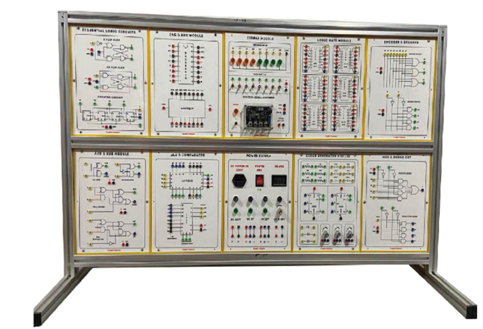
- Combinational Logic Circuit Experiment
- Arithmetical Logic/Tri-state & Code Converter Experiment
- Encoder, Decoder & Multiplexer Logic Circuit Experiment
- Flip-flop & Sequential Logic & Counter Circuit Experiment
- Oscillator/Pulser ; Load ; Up/Down Counter Circuit Experiment
- Memory ; Matrix LED ; DAC/ADC & MCU Interface Circuit Experiment
- Digital & Analog Timer ,Pulse Generator Circuit Experiment
- Ramp-compare/SAR/Dual-slope ADC Experiment
- Keyboard & Display for Stepping Motor Position Control
- Precise Digital Clock Timer
- Universal CPLD & Breadboard Experiment
List of Experiments
- Combinational Logic Circuit Experiment
(1) NOR gate circuit
(2) NAND gate circuit
(3) XOR gate circuit
- Constructing XOR gate with NAND gate
- The combination with basic gates
(4) AND-OR-INVERTER (A-O-I) gate circuit
(5) Comparator circuit
- Comparator constructed with basic logic gates
- Comparator constructed with TTL IC
(6) Schmitt gate circuit
(7) Open-collector gate circuit
- High voltage/current circuit
- Constructing an AND gate with open-collector gate
(8) Half-adder and full-adder circuit: Construct HA with basic logic gates
(9) Half-subtractor and full-subtractor circuit: Subtractor circuit constructed with basic logic gates
(10) Bit parity generator circuit: Bit parity generator constructed with XOR gates
(11) Constructing a 4-to-10 decoder with TTL IC
(12) The switch characteristics of TTL level conversion circuit
- Arithmetical Logic/Tri-state & Code Converter Experiment
(1) CMOS FET tristate gate circuit
- Truth table measurements
- Constructing an AND gate with tristate gate
- Bidirectional transmission circuit
(2) Half-adder and full-adder circuit
- Full-adder circuit with IC
- High-speed adder carry generator circuit
- BCD code adder circuit
(3) Half-subtractor and full-subtractor circuit: Full-adder and inverter circuit
(4) Arithmetic Logic Unit (ALU) circuit
(5) Bit parity generator circuit: Bit parity generator IC
(6) Hex to Dec/Dec to Hex digital conversion
- 8-digit Dec-to-Hex conversion
- 8-bit Hex-to-Dec conversion
- Encoder, Decoder & Multiplexer Logic Circuit Experiment
(1) Encoder circuit
- Constructing a 4-to-2 encoder with basic gates
- Constructing a 9-to-4 encoder with TTL IC
(2) Decoder circuit
- Constructing a 2-to-4 decoder with basic gates
- BCD-to-7-segment decoder
(3) Multiplexer circuit
- Constructing a 2-to-1 multiplexer
- Using multiplexers to create functions
- Constructingan 8-to-1 multiplexer circuit with TTL IC
(4) Demultiplexer circuit: Constructing a 2-output demultiplexer with basic logic gates
(5) Digitally controlled analog multiplexer/demultiplexer circuit
(6) The switch characteristics of CMOS level conversion circuit
- Flip-flop & Sequential Logic & Counter Circuit Experiment
(1) Flip-flop circuits
- Construct R-S flip-flop with basic logic gates
- Construct D flip-flop with R-S flip-flops
- Construct noise elimination circuit with R-S flip-flops
- Construct J-K flip-flop with D flip-flops
- The J-K flip-flop of delay and differential
f . Construct master-slave J-K flip-flops with dual R-S flip-flops
- Construct shift register with D flip-flops
- Preset left/right shift register
(2) J-K flip-flop counters
- Asynchronous binary up counter
- Asynchronous binary down counter
- Asynchronous decade up counter
- Synchronous binary counter
- Synchronous binary up counter
f . Synchronous binary up/down counter
- Johnson counter
- Ring counter
- Oscillator/Pulser ; Load ; Up/Down Counter Circuit Experiment
(1) Constructing Random Access Memory (RAM) with D flip-flop
(2) 64-bit Random Access Memory (RAM) circuit
(3) Erasable Programmable Read Only Memory (EPROM) circuit
(4) Asynchronous four-bit binary up counter (use of 7493 IC)
(5) Presentable binary up/down counter
(6) Presentable decimal up/down counter
(7) Construct Non-retrigger able circuit with the specialized CMOS IC
(8) Construct refrigerable circuit with CMOS IC
(9) Construct a variable duty cycle oscillator circuit with dual monostablemultivibrators
- Memory, Matrix LED & DAC/ADC & MCU Interface Circuit Experiment
(1) Electronic EPROM (EEPROM) circuit
(2) DAC0800 unipolar conversion circuit experiments
(3) Bipolar output conversion circuit
(4) ADC0804 8-bit SAC analog-to-digital converter experiment
(5) Constructing dynamic scanning counter with singlechip microprocessor
- Digital & Analog Timer, Pulse Generator Circuit Experiment
(1) Constructing oscillator circuit with basic logic gates
- Resistor-capacitor multivibrator
- Resistor-capacitor crystal multivibrator
(2) Constructing oscillator circuit with Schmitt gate
- Resistor-capacitor oscillator
- Variable duty cycle resistor-capacitor oscillator
(3) 555 IC oscillator circuit
- 555 oscillator circuit
- Voltage controlled oscillator circuit
(4) Monostablemultivibrator circuits
- Low-speed monostablemultivibrator circuits
- Monostable ON/OFF delay circuit
- Monostable ON/OFF timer circuit
- Construct monostablemultivibrator circuit with 555 IC
(5) Numerically-Controlled Oscillator (NCO) signal generator
(6) Precise-frequency function generator
(7) Variable-duty-cycle NCO signal generator
(8) Variable-ON/OFF delay and difference control experiments
(9) Precise 15-bit symmetric/asymmetric PWM generator
- Ramp-compare/SAR/Dual-slope ADC Experiment
(1) Simple R-2R unipolar output D/A converter experiments
(2) 8-bit digital-ramp A/D converter experiment
(3) 8-bit successive-approximation A/D converter experiment
(4) 8-bit dual-slope A/D converter experiment
- Keyboard & Display for Stepping Motor Position Control
(1) Stepper motor position/speed control experiment
- Precise Digital Clock Timer
(1) Clock experiment
(2) Timer experiment
- Universal CPLD & Breadboard Experiment
(1) Create block diagram/schematic file in QUARTUS
(2) 16-bit Hex counter
(3) 16-bit decimal counter
(4) 16-bit presentable decimal up/down counter
(5) 16-bit scanning controller for 7-segment display
(6) 16-bit up/down counter and its indication by a 7-segment display
(7) Electronic music box
(8) The traffic light with animation and time indication
Interfacing Software: QUARTUS II Web Edition
-Built-in circuit simulation of experiment modules.
-Fault simulation is allowed.
-Users can flexibly compare the simulation analysis result with hardware signal output.
-Support virtual instrument.
Accessories-1
- Experiment Manual and Instructor’s Manual
- Connection Leads and Plugs
- Key
Accessories-2
- Experiment Manual
- Connection Leads and Plugs
- USB-Blaster
Additional Accessories:
- Power Cord: 01 No
- Connecting Wire & Cable
- Complete 5 days Training Included
- User Manual or User Guide
Protection:
Under voltage, Supply and DC Link overvoltage, Phase loss, Drive overload, Instantaneous,Over current, short circuit, Ground fault, etc.


Reviews
There are no reviews yet.